6-Instruction CPU
一、CPU 結構圖
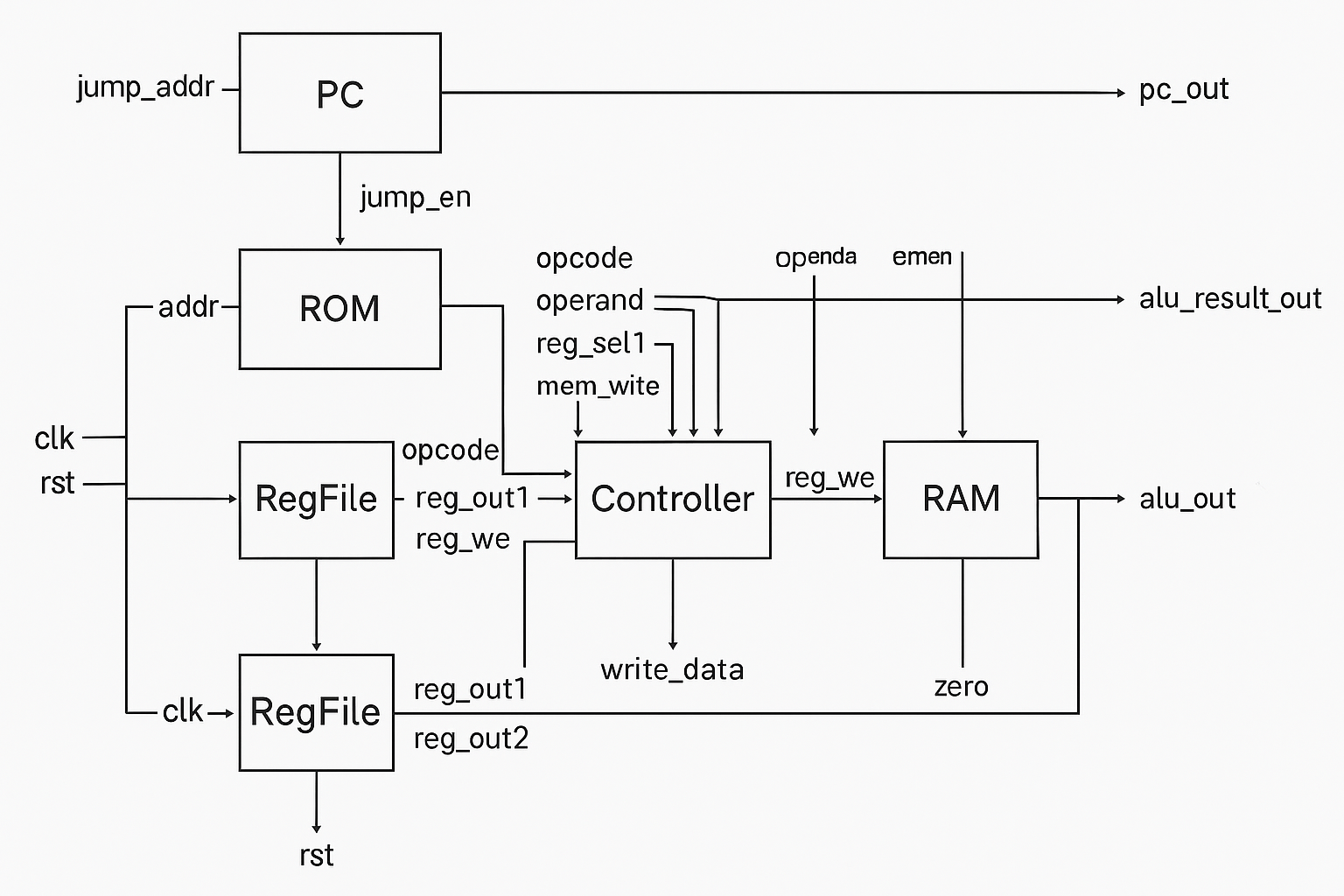
註:CPU 結構採單週期架構,所有模組皆於一個時脈週期內完成。
二、指令集說明
| Opcode | 指令名稱 | 格式 | 功能說明 |
|---|---|---|---|
| 000 | LOADI | LOADI Rx, Imm | 將立即數寫入暫存器 Rx |
| 001 | LOAD | LOAD Rx, [Addr] | 從記憶體讀取資料至 Rx |
| 010 | STORE | STORE Rx, [Addr] | 將 Rx 的資料寫入記憶體 |
| 011 | ADD | ADD Rx, Ry | Rx = Rx + Ry |
| 100 | SUB | SUB Rx, Ry | Rx = Rx - Ry |
| 101 | JMP | JMP Addr | 跳躍至位址 Addr |
| 110 | JZ | JZ Addr | 若 Zero flag = 1 則跳至 Addr |
Rx, Ry 為暫存器 R0–R3,Addr 與 Imm 為 5 位元。
三、模組設計說明
1. 頂層模組(cpu)
負責整合各個模組,控制資料流與時脈推進。
module cpu (
    input clk,
    input rst,
    output [7:0] pc_out,
    output [7:0] alu_result_out
);
    // 暫存線路
    wire [7:0] pc;
    wire [7:0] instr;
    wire [2:0] opcode;
    wire [4:0] operand;
    wire [7:0] alu_out;
    wire [7:0] reg_out1, reg_out2;
    wire [1:0] reg_sel1, reg_sel2;
    wire [7:0] ram_out;
    wire mem_write;
    wire zero_flag;
    wire reg_we;
    wire [7:0] write_data;

    assign pc_out = pc;
    assign alu_result_out = alu_out;
    assign write_data = (opcode == 3'b000) ? {5'b00000, operand[2:0]} : alu_out;

    // 模組實例化
    pc pc_unit(
    .clk(clk),
    .rst(rst),
    .jump_addr({3'b000, operand}),
    .jump_en((opcode == 3'b101) || ((opcode == 3'b110) && zero_flag)),
    .pc(pc)
    );
    rom rom_unit(.addr(pc), .data(instr));
    controller controller_unit(
        .instr(instr),
        .opcode(opcode),
        .operand(operand),
        .reg_sel1(reg_sel1),
        .reg_sel2(reg_sel2),
        .mem_write(mem_write),
        .reg_we(reg_we)
    );
    regfile regfile_unit(
        .clk(clk),
        .rst(rst),
        .we(reg_we),
        .ra(reg_sel1),
        .rb(reg_sel2),
        .wd(write_data),
        .a_data(reg_out1),
        .b_data(reg_out2)
    );
    alu alu_unit(.a(reg_out1), .b(reg_out2), .op(opcode), .y(alu_out), .zero(zero_flag));
    ram ram_unit(.clk(clk), .addr(operand[3:0]), .we(mem_write), .din(reg_out1), .dout(ram_out));
endmodule
2. PC(程式計數器)
維護目前指令位址,支援條件跳躍。
module pc (
    input clk,
    input rst,
    input [7:0] jump_addr,
    input jump_en,
    output reg [7:0] pc
);
    always @(posedge clk or posedge rst) begin
        if (rst) pc <= 0;
        else if (jump_en) pc <= jump_addr;
        else pc <= pc + 1;
    end
endmodule
3. ROM
初始化指令集,僅讀取不寫入。
module rom (
    input [7:0] addr,
    output reg [7:0] data
);
    reg [7:0] memory [0:255];
    integer i;

    initial begin
        for (i = 0; i < 256; i = i + 1)
            memory[i] = 8'b000_00_000;  // 預設 NOP

        memory[0] = 8'b000_00_001; // LOADI R0, 1
        memory[1] = 8'b000_01_010; // LOADI R1, 2
        memory[2] = 8'b011_00_010; // ADD R0 += R1
        memory[3] = 8'b010_00_001; // STORE R0 → RAM[1]
        memory[4] = 8'b000_10_011; // LOADI R2, 3
        memory[5] = 8'b000_11_011; // LOADI R3, 3
        memory[6] = 8'b100_10_110; // SUB R2 -= R3
        memory[7] = 8'b110_01000;  // JZ to 8
        memory[8] = 8'b000_00_111; // LOADI R0, 7 (should be skipped)
        memory[9] = 8'b001_11_001; // LOAD R3 ← RAM[1]
        memory[10]= 8'b101_01010;  // JMP loop HALT (to address 10)
    end

    always @(*) begin
        data = memory[addr];
    end
endmodule
4. RAM
資料記憶體,可寫入或讀取。
module ram (
    input clk,
    input [3:0] addr,
    input we,
    input [7:0] din,
    output reg [7:0] dout
);
    reg [7:0] mem [0:15];
    always @(posedge clk) begin
        if (we)
            mem[addr] <= din;
        dout <= mem[addr];
    end
endmodule
5. Controller
解析指令並輸出控制訊號(opcode、reg_we、mem_write、jump_en)。
module controller (
    input [7:0] instr,
    output [2:0] opcode,
    output [4:0] operand,
    output [1:0] reg_sel1,
    output [1:0] reg_sel2,
    output mem_write,
    output reg_we,
    output jump_en_conditional
);
    assign opcode = instr[7:5];
    assign operand = instr[4:0];
    assign reg_sel1 = instr[4:3];
    assign reg_sel2 = instr[2:1];
    assign mem_write = (opcode == 3'b010); // STORE

    assign reg_we =
        (opcode == 3'b000) || // LOADI
        (opcode == 3'b001) || // LOAD
        (opcode == 3'b011) || // ADD
        (opcode == 3'b100);   // SUB

    assign jump_en_conditional = (opcode == 3'b110); // JZ
endmodule
6. RegFile
四組暫存器(R0–R3),支援雙讀單寫。
module regfile (
    input clk,
    input rst,
    input we,
    input [1:0] ra,
    input [1:0] rb,
    input [7:0] wd,
    output [7:0] a_data,
    output [7:0] b_data
);
    reg [7:0] regs [0:3];
    assign a_data = regs[ra];
    assign b_data = regs[rb];
    always @(posedge clk or posedge rst) begin
        if (rst) begin
            regs[0] <= 0;
            regs[1] <= 0;
            regs[2] <= 0;
            regs[3] <= 0;
        end else if (we) begin
            regs[ra] <= wd;
        end
    end
endmodule
7. ALU
支援加法、減法運算,輸出 zero flag。
module alu (
    input [7:0] a,
    input [7:0] b,
    input [2:0] op,
    output reg [7:0] y,
    output zero
);
    always @(*) begin
        case (op)
            3'b011: y = a + b;     // ADD
            3'b100: y = a - b;     // SUB
            default: y = 8'd0;
        endcase
    end
    assign zero = (y == 0);
endmodule
四、模擬與測試
測資指令(ROM 中)
memory[0] = 8’b000_00_001; // LOADI R0, 1
memory[1] = 8’b000_01_010; // LOADI R1, 2
memory[2] = 8’b011_00_010; // ADD R0 += R1
memory[3] = 8’b010_00_001; // STORE R0 → RAM[1]
memory[4] = 8’b000_10_011; // LOADI R2, 3
memory[5] = 8’b000_11_011; // LOADI R3, 3
memory[6] = 8’b100_10_110; // SUB R2 -= R3
memory[7] = 8’b110_01000; // JZ to 8
memory[8] = 8’b000_00_111; // LOADI R0, 7 (should be skipped)
memory[9] = 8’b001_11_001; // LOAD R3 ← RAM[1]
memory[10]= 8’b101_01010; // JMP loop HALT (to address 10)
模擬結果波形圖
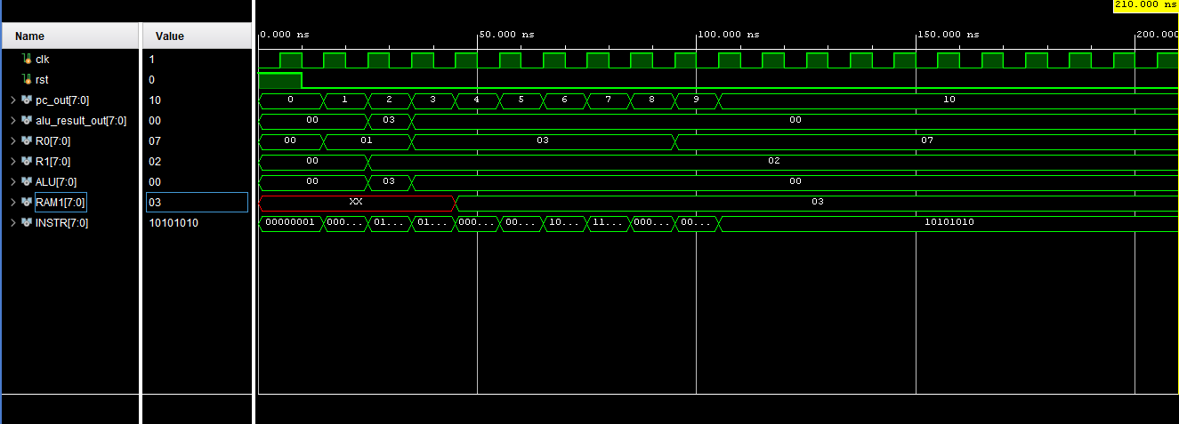
測試重點
- LOADI 正確寫入 R0, R1
- ADD 成功相加
- STORE 寫入 RAM[1]
- SUB 結果為零時觸發 JZ
- LOAD 成功將 RAM[1] 讀至 R3
五、結論與心得
本次專題完成一顆自訂 6 指令 CPU,並以模組化方式建構。過程中理解 CPU 單週期架構的資料流與控制流,熟悉 Verilog 行為式設計與模擬技巧,成功驗證各種運算與跳躍邏輯。後續若擴充指令集或導入 pipeline,可參考本架構進行微調。